What is MIP LED Screen? Technology, Advantages & Applications
MIP LED technology is transforming the future of fine-pitch LED displays.
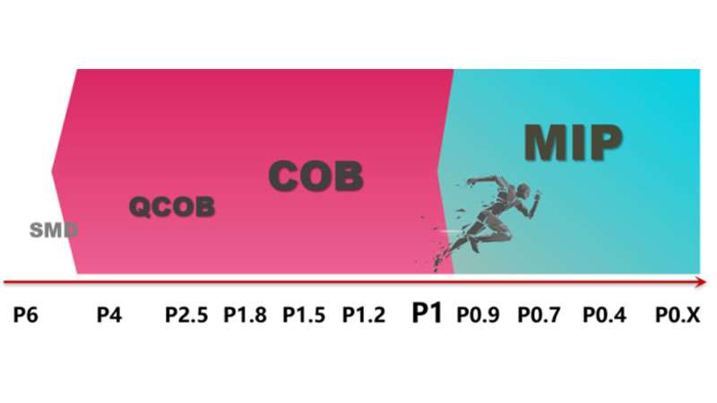
The LED display industry has evolved from DIP to SMD and then to COB packaging technologies, each delivering improvements in pixel pitch, resolution, and reliability. However, as the market demands ultra-fine pitch LED displays for XR studios, cinemas, and home theaters, existing technologies face limitations.
MIP LED display has emerged as a breakthrough, bridging the gap between cutting-edge Micro LED performance and scalable mass production. This post explores what MIP LED is, how it works, its advantages over COB and SMD, and where it is applied.
Table of Contents
1. What is MIP LED Technology?
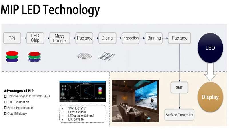
MIP LED, or Micro LED in Package, is an advanced packaging method that enables the mass production of fine pixel pitch LED displays. Unlike COB (Chip on Board) technology, where bare LED chips are directly bonded onto the substrate, MIP encapsulates each Micro LED chip into a standardized package before mounting it onto the PCB using SMT (Surface Mount Technology).
This approach combines the superior performance of Micro LEDs, such as high brightness, low power consumption, and long lifespan, with the scalability and repairability of traditional SMD processes.
During manufacturing, Micro LED wafers are cut into tiny chips, tested for quality, and then sealed into protective packages. These packaged LEDs can be efficiently assembled with existing SMT equipment, making MIP highly compatible with current production lines.
The result is a display solution that offers better production yield, higher durability, and easier maintenance compared to COB. Moreover, MIP supports ultra-fine pixel pitches down to P0.4–P0.9, enabling true 4K and 8K visuals for next-generation applications.
2. How MIP LED Screen Works?
A MIP LED screen operates by integrating Micro LED chips that have been pre-packaged into standardized units, which are then assembled on printed circuit boards through Surface Mount Technology (SMT). This process combines the advantages of Micro LEDs with the practicality of mass production.
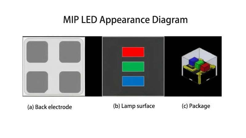
Each Micro LED chip is first encapsulated into a protective package that safeguards it from dust, moisture, and external stress. These packaged LEDs are then sorted and color-matched to ensure uniform brightness and wavelength. Once mounted onto the PCB, millions of these tiny light-emitting diodes work together as pixels, forming the high-resolution image of the display.
Because every packaged LED emits its own red, green, or blue light, the screen achieves true self-emissive performance with exceptional contrast and wide viewing angles. Compared with COB, which bonds bare chips directly, MIP allows for easier repair and replacement, since individual LED packages can be swapped out if damaged.
In essence, a MIP LED screen works like a highly refined version of SMD, but with the added precision and scalability of Micro LED technology.
3. Advantages & Disadvantages of MIP Packaging Technology
Like any emerging technology, MIP LED packaging brings clear benefits but also faces certain challenges.
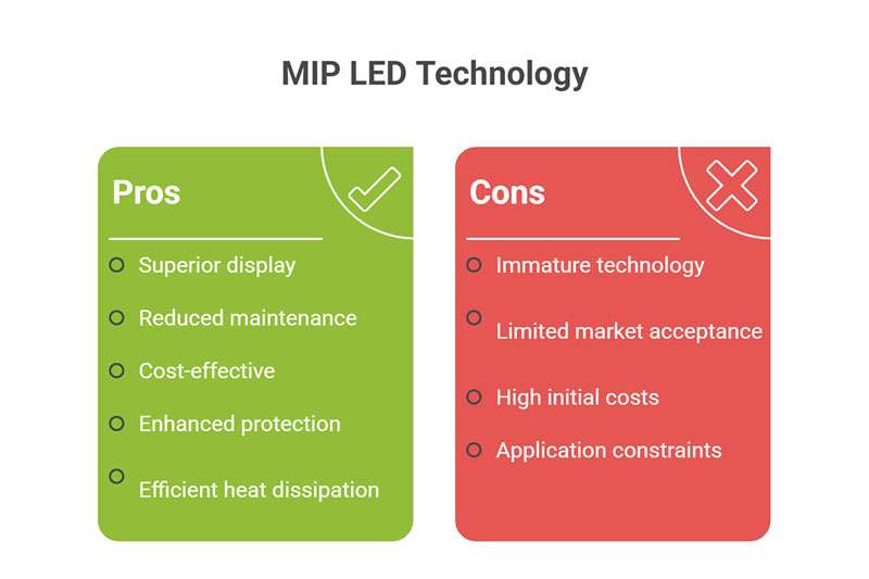
Advantages:
MIP LED, as an innovative packaging technology, seamlessly integrates LED chips with discrete components, bringing new possibilities and advantages to Micro LED displays.
- Lower maintenance requirements
First, if a defective lamp is detected in an LED screen using MIP packaging, it can be removed and replaced individually without affecting other components on the screen.
Furthermore, LED panels based on MIP technology achieve uniform color quality, excellent light separation and color mixing, and require no subsequent calibration or maintenance.
Compared to traditional LED packaging technologies, MIP packaging requires significantly less ongoing maintenance.
- Lower maintenance costs
Traditional COB technology places very stringent requirements on Mini LED chips, forcing upstream chip manufacturers to invest excessively in optical separation, color separation, and material mixing. MIP packaging, however, enables mass production and reduces wafer costs.
MIP packaging can effectively reduce the rate of defective product screening and lower downstream rework costs.
- Better display quality
MIP packaging enables comprehensive measurement of Micro RGB pixels, providing precise and detailed spectrophotometry. Experimental verification has shown that LED lamps packaged with MIP LED technology exhibit excellent brightness, contrast ratio, and color consistency across various viewing angles.
- Excellent Protection
MIP packaging provides LED devices with excellent dust, moisture, and static protection, providing better resistance to external forces.
- Excellent Protection
LED modules packaged with MIP technology offer improved heat dissipation, resulting in lower power consumption and temperature rise.
Disadvantages:
Technology Maturity
Although MIP technology offers significant advantages, its maturity level is still behind traditional methods. Challenges remain in areas such as mass transfer, color binning, and yield control, requiring continuous R&D and process optimization.
Market Acceptance
As an emerging LED package technology, MIP packaging technology still needs time to gain broader market adoption. Both users and industries require more time to fully understand, validate, and trust its advantages in display performance, reliability, and value.
Cost Competitiveness
In certain high-end applications, the cost advantage of MIP packaging is not yet fully realized. Compared with established packaging methods, further breakthroughs are needed in reducing production costs and improving cost-performance ratios.
Application Limitations
While MIP excels in fine-pitch LED displays, it still faces challenges in some specialized scenarios. For example, in cases requiring ultra-high pixel density, MIP may need to be combined with other packaging technologies to meet diverse application requirements.
4. Technological Innovation: Core Competitiveness of MIP LED
The technological innovations of MIP LEDs are reflected in multiple dimensions, demonstrating strong competitiveness in packaging processes, manufacturing efficiency, and display performance.
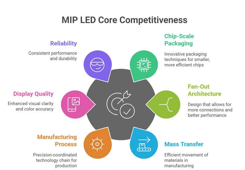
① Chip-Scale Packaging and Fan-Out Architecture Innovation
MIP LED screens utilize fan-out packaging technology. By rewiring the Micro LED chip pins, the pins are enlarged, making the pad size easier to mount. This innovative design directly reduces the precision requirements of the PCB substrate (compared to COB technology).
② Mass Transfer and Efficient Manufacturing Process
In terms of manufacturing efficiency, MIP LEDs utilize laser mass transfer technology, capable of transferring tens of thousands of light-emitting chips per minute with an accuracy of ±5μm. This significant increase in production efficiency has the potential to reduce unit manufacturing costs.
③ Improved Display Quality and Reliability
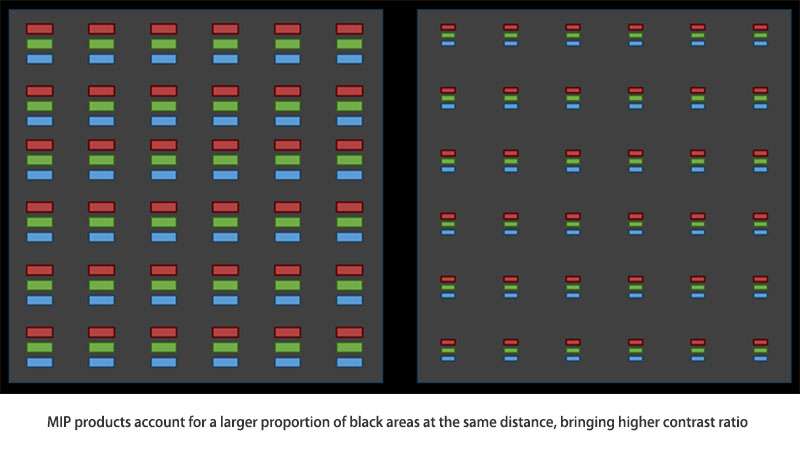
MIP LED screens also excel in display quality. Full pixel measurement and sorting technology ensures consistent brightness and color temperature. A black gel filling process reduces optical crosstalk and, combined with high-transmittance silicone, significantly improves light efficiency.
Furthermore, the micro-level light-emitting chips used in MIP are smaller than traditional COB chips, resulting in a higher proportion of black areas, further enhancing the blackness of the panel’s ink color and delivering a more striking visual experience.
④ Manufacturing Process: A Precision-Coordinated Technology Chain
The manufacturing process for MIP devices is closely linked:
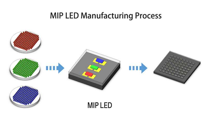
- First, mass transfer is performed, transferring Micro LED chips (sub-50 micron) to a substrate to form an array;
- Next, fan-out packaging is performed, enlarging the electrode pins through semiconductor processing;
- Next, dicing and sorting are performed, cutting the packaged substrate into individual discrete devices and testing their optoelectronic performance;
- Finally, a die bonder is used to transfer the chips to a PCB or glass substrate. Each step demonstrates the precision and rigor of the technology.
5. Applications of MIP LED Displays
Thanks to its unique balance of high performance, fine pixel pitch, and scalability, MIP LED display technology is being adopted across a wide range of industries.
|
Application Scenarios |
Description |
| Command and Control Centers | MIP LED displays provide ultra-clear visualization for mission-critical environments. The fine pixel pitch enables operators to analyze complex data, maps, and video feeds with absolute precision. |
| Broadcast and XR Studios | Virtual production and extended reality demand seamless backgrounds with minimal moiré and excellent color accuracy. MIP LEDs deliver lifelike visuals, making them a top choice for modern studios. |
| Corporate and Education | High-end boardrooms, lecture halls, and conference centers use MIP LED video walls for impactful presentations and immersive learning experiences, benefiting from their reliability and sharp resolution. |
| Luxury Home Theaters | With pixel pitches under P1.0, MIP LED screens bring true cinema-quality visuals into private residences, supporting 4K and 8K playback with deep contrast and wide viewing angles. |
| Retail and Public Spaces | Premium retail stores and exhibitions use MIP LED for vibrant digital signage, capturing attention with stunning brightness and color uniformity. |
|
Medical Imaging and Simulation |
The ultra-fine detail provided by MIP LEDs makes them suitable for medical visualization and advanced training simulations where accuracy is critical. |
In essence, MIP LED displays are redefining visual standards across industries that demand precision, scalability, and next-generation quality.
6. MIP vs COB vs SMD LED Display
To better understand the unique value of MIP LED screen, it helps to compare it with two mainstream packaging technologies: COB (Chip on Board) and SMD (Surface Mounted Device) LED screens.
Learn more about SMD vs COB here.
| Feature | MIP LED | COB LED | SMD LED |
| Pixel Pitch | Ultra-fine (P0.4 – P0.9) | Fine (P0.4 – P1.2) | Medium to large (P1.2 – P10) |
| Maintenance | Easy – individual LED packages are replaceable | Difficult – faulty chips are harder to repair | Easy – replaceable modules |
| Durability | Strong, encapsulated protection against dust & moisture | Vulnerable, chips exposed to the environment | Good, but less durable than MIP |
| Visual Quality | Excellent uniformity, HDR-ready | Excellent contrast, smooth surface | Good, but limited at small pitches |
| Scalability | Compatible with SMT mass production | Limited, requires a stricter environment | Widely scalable, standard process |
| Best Use Cases | XR studios, control rooms, luxury theaters | Premium fine-pitch indoor displays | Outdoor, rental, general indoor |
https://youtu.be/_-2dkXX85vg?si=875wlWI3lAP__rmfhttps://youtu.be/PLq_byBkD7Y?si=NHLT1KaoBJeV9bBk
Key Insights:
- MIP vs COB: Both support fine-pitch displays, but MIP has higher yield and easier maintenance, while COB offers seamless surface integration.
- MIP vs SMD: SMD is cost-effective and widely used for larger pixel pitches, but it cannot achieve the same fine detail as MIP.
MIP LED screen combines the reliability of SMD with the performance of COB, making it the most promising path for next-generation Micro LED displays.
7. Future Trends in MIP LED Display Technology
As the demand for ultra-fine pitch LED displays continues to rise, MIP LED technology is expected to play a central role in shaping the future of the display industry. By combining Micro LED’s high performance with scalable packaging and SMT compatibility, MIP offers a clear pathway toward mass adoption.
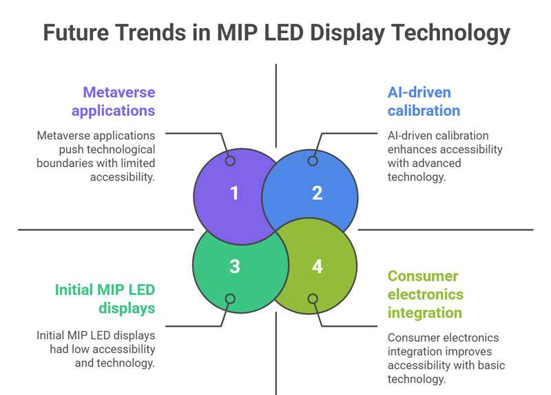
One key trend is the continued miniaturization of pixel pitch. With MIP already supporting P0.4–P0.9, future developments will push the boundaries even further, enabling 8K and beyond on medium-sized screens. This opens opportunities in areas such as metaverse environments, AR/VR applications, and next-generation home theaters.
Another major trend is improved manufacturing efficiency. As packaging equipment evolves and yield rates increase, the cost barrier for Micro LED displays will gradually decrease, making MIP LEDs more accessible to broader markets, from high-end commercial use to consumer electronics.
In addition, MIP will likely integrate with AI-driven calibration and modular design innovations, enabling smarter maintenance, self-adjusting brightness, and even easier pixel-level repair. This enhances both long-term performance and sustainability.
Finally, MIP is positioned to expand into diverse industries, from automotive displays to medical imaging, thanks to its durability, high brightness, and energy efficiency.
8. FAQs
1. How does MIP differ from COB and SMD?
MIP combines the durability and repairability of SMD with the fine-pitch performance of COB. Compared to COB, it offers higher production yield and easier maintenance; compared to SMD, it enables much smaller pixel pitches.
2. Are MIP LED screens easy to maintain?
Yes. Since each Micro LED is packaged individually, defective LEDs can be replaced without reworking the entire module, unlike COB.
3. Do MIP LED screens support HDR?
Yes. With high brightness, excellent contrast, and precise color matching, MIP LED screens are fully compatible with HDR content.
4. Are MIP LED screens expensive?
Currently, they are more costly than SMD displays, but prices are expected to drop as manufacturing yield improves and adoption scales.
5. Can MIP LED be used outdoors?
While primarily designed for indoor fine-pitch applications, MIP LEDs with protective encapsulation can also be adapted for semi-outdoor environments.
9. Conclusion
MIP LED is revolutionizing the LED display industry by combining Micro LED performance with mass-production feasibility. It delivers higher yield, better durability, and superior visual performance compared to SMD and COB.
With applications in XR production, cinemas, control rooms, and luxury home theaters, the MIP LED screen is rapidly gaining traction as the future of fine-pitch LED displays.
Related Posts
wp:paragraph
/wp:paragraph